ARM Core Dataflow Model
The article deals with the explanation of the ARM core dataflow model. It also covers the complete implementation of architecture of the ARM processor(Complete ARM series ).

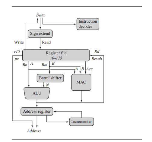
As depicted in figure, an ARM core dataflow model may be thought of as functional units connected by data buses, with the arrows representing data flow, the lines representing buses, and the boxes representing either an operating unit or a storage region. The diagram depicts both the data flow and the abstract components that make up an ARM core. The Data bus is where data enters the CPU core. The data might be an executable command or a data object. The ARM is implemented by Von Neumann in figure, with data items and instructions sharing the same bus. The ARM implementations at Harvard, on the other hand, employ two separate buses. Before instructions are executed, the instruction decoder interprets them.Each instruction that is executed is part of a certain instruction set.
The load-store architecture is used by the ARM processor, as it is by all RISC processors. This implies there are two sorts of instructions for moving data in and out of the processor: load instructions copy data from memory to core registers, while store instructions copy data from registers to memory. Data processing instructions that directly manipulate data in memory are not available. As a result, data processing is limited to registers. The register file—a storage bank made up of 32-bit registers—is where data objects are stored. Most instructions consider the registers as having signed or unsigned 32-bit values since the ARM core is a 32-bit processor.
When signed 8-bit and 16-bit integers are read from memory and stored in a register, the sign extend hardware transforms them to 32-bit values. Rn and Rm are the two source registers of ARM instructions, while Rd is the result or destination register. The internal buses A and B are used to read source operands from the register file. The ALU (arithmetic logic unit) or MAC (multiply-accumulate unit) computes a result using the Rn and Rm register values from the A and B buses. The outcome of data processing instructions is written directly to the register file in Rd. The ALU is used in load and store instructions to create an address that is stored in the address register and broadcast over the Address bus. Because the ARM7 architecture is based on the von Neuman architecture, the same bus is used to load both instructions and data.
As a result, the input data bus is linked to
• Direct Register bank
• Sign extend hardware block
• Instruction decode Block
Click here to read about ARM registers
Register Bank in ARM Processor
The ARM architecture has a load store architecture, which means that any processor unit may process data stored in registers. As a result, data must be entered into the register bank.
The register file is a storage bank made up of 32-bit registers, where data objects are stored.
Most instructions consider the registers as having signed or unsigned 32-bit values since the ARM core is a 32-bit processor. When signed 8-bit and 16-bit integers are read from memory and stored in a register, the signed extended hardware transforms them to 32-bit values.
Register file contains
• General purpose registers, which are used by ALU/MAC.
• Program Counter (r15 register), hence it is connected to the address register too.
Basic processing unit are
ALU (Arithmetic and Logical Unit)
ALU is designed to conduct mathematical operations such as add, sub, etc., as well as logical operations such as OR/AND, etc., on data stored in data registers.
Barrel shifter
A barrel shifter is a digital circuit capable of shifting a data word by a specific number of bits in a single clock cycle. This hardware unit can execute data shifting operations on the data in the register bank.
MAC (Multiply and accumulate unit)
Basic summation operations on data in registers are supported.
Any operation’s result can be written back to the register bank, or if the instruction needs memory access, the result is sent to the address register.
Address register
This contains the address from which data or instruction needs to be fetched.
This register is connected to an incrementing unit.
What is ARM Architecture – ARM Core Dataflow Model
Although an ISA version may have several processor implementations, each ARM processor implementation executes a single instruction set architecture .
To keep up with the demands of the embedded industry, the ISA has been developed. ARM has carefully regulated this evolution to ensure that code built for an older architecture revision would also run on a later architecture revision.
We must first define the ARM processor nomenclature before moving on to illustrate the architecture’s development. Individual processors are identified by the nomenclature, which also offers basic information about the feature set.

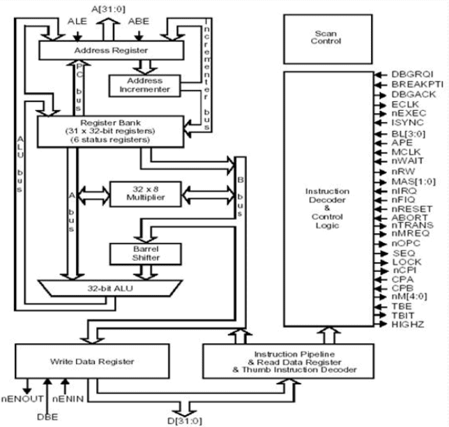
Internal Architecture of ARM7
- Von Neumann Architecture
- 3-stage pipeline
- 32-bit Data bus
- 32-bit Address bus
- 37 32-Bit Registers
- 32-bit ARM instruction Set
- 16-Bit Thumb instruction Set
- 32×8 Multiplier
Reference – www.arm.com/architecture/cpu
