Introduction to Attiny85
ATtiny85, introduced by Microchip is an 8-bit microcontroller having high performance. It has many good features in its small size. It is based on RISC CPU architecture. It is compact in size and has 8-kBytes of in-system programmable flash. As it falls under the category of low-power controller, it proves to be a better fit for real-time applications which can work on minimum power. It can execute powerful instructions in a single clock cycle, so Attiny85 is able to cross the throughput of 1 MIPS per MHz. This helps the designers to optimize power consumption with respect to processing speed.
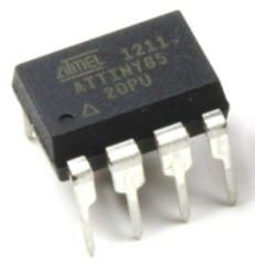
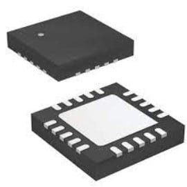
As shown in the figure, this is available in various types of packages such as PDIP, SOIC, TSSOP: these have 8 pin interface and QNF has 20 pin interface.
Attiny85 Features
- Architecture: Advanced RISC.
- Flash memory: 8 kilobytes: 10000 writes/erase cycles.
- CPU speed: 1 MIPS at 1 MHz.
- Registers: 32
- Operating Voltage: On 1.8V, current consumption is 300 uA.
- Power down mode: On 1.8V, current consumption is 0.1 uA.
- RAM: 512 bytes on internal SRAM.
- EEPROM: 512 bytes of in-system programmable EEPROM.
- Operating Temperature: -55 ℃ to +125 ℃.
- Total Pins: 8
- Total I/O pins: 6
- Minimum Operation Voltage: 1.8V DC; Maximum Operating Voltage: 5.5V DC.
- ADC: 4 channels, 10-bit resolution ADC.
- Modes: three modes: Idle, ADC Noise reduction, power-down.
- Serial Peripheral Interface: Available
- Program Lock: Available.
- Watchdog Timer: Available
Attiny85 Pinout
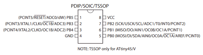
| Pin number | Pin Name | Pin Function/Description |
| 1 | PB5 | This pin is a reset pin, analog pin, ADC input, bootloader reprogram. |
| 2 | PB3; GPIO3 | Function of this is for USB programming; analog input; XTAL input; PWM. |
| 3 | PB4; GPIO4 | Function of this is for USB programming; analog input; XTAL input; PWM. |
| 4 | GND | This pin is used to provide Ground/Negative supply to the system. |
| 5 | PB0; GPIO0 | This pin functions as PWM output; SPI communication; 12C communication. |
| 6 | PB1; GPIO1 | This pin can be used as SPI data output; PWM output. |
| 7 | PB2; GPIO2 | This pin is for analog output; SPI data and SCL. |
| 8 | VCC | This pin is used to provide a Positive supply to the system. |
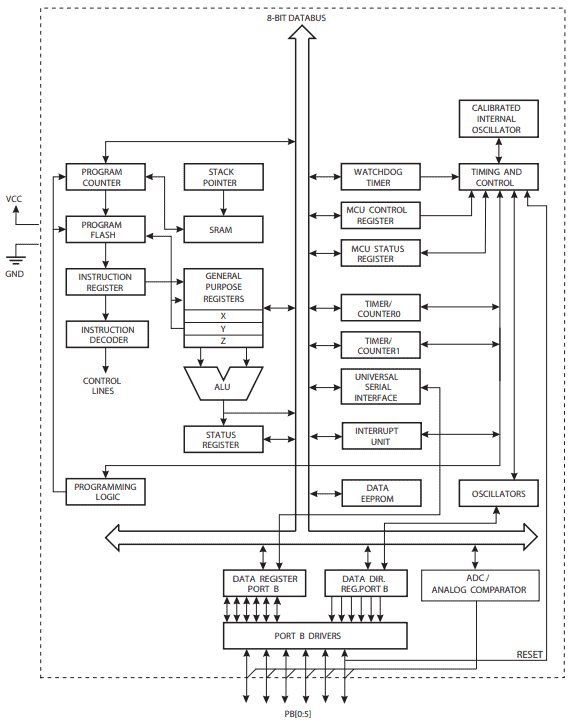
Attiny85 Block Diagram
The given block diagram helps to visualize the main functions of the controller and how the components are connected to each other.
Functions
It can perform various functions on this single chip. As described earlier, some of the pins are used for more than one purpose.
- Timers: The chip has two timers in it which help certain functions when run on timer mode generates a delay in the process. Moreover, these timers also count the number of intervals for a certain function when used in counter mode. The timer mode is used to increase the instruction cycle whereas the counter mode is used to increase the rising and falling edge of the pin.
- SPI communication: As ATtiny85 comes with Serial Peripheral Interface (SPI), It is mainly responsible for establishing the communication between various connected peripheral devices such as SD cards, sensors and shift registers. It separates clock and data lines and the select line to pick the required appropriate device for communication. This connection allows both the linked devices to use the same communication protocol to set out the same channel of communication.
- I2C Communication: The I2C protocol, which is primarily a two-wire protocol used to link low-speed devices such as ADC and DAC converters, I/O interfaces, and microcontrollers, is included in the device. The essential components of this communication protocol are the two wires known as Serial Clock (SCL) and Serial Data (SDA).
- Brown Out Reset (BOR): As soon the voltage supply drops below the brownout threshold voltage, BOD resets the controller. Therefore, to secure the controller due to a power drop in the voltage line, various voltage ranges are provided.
- Interrupt: During an emergency, Interrupt comes in the role which puts the main executing function on hold and helps the requires instructions to execute which are necessary during that time. After the interrupt (required instructions) is executed completely, the running code puts the controller back to the main program.
- ADC converter: The ADC module is a useful addition to the system that allows it to communicate with sensors. It is a 10-bit module with 4 channels, which is slightly fewer than the number of channels available on Microchip modules, which typically have 7 or 12 channels.
Applications
- ATtiny85 is used in various technical engineering projects (Embedded System Projects) based on requirements.
- Weather Sensor Systems
- Used in IoT applications
- Industrial Automation
- Robotics
- Solar Applications
- Security and Automobile based applications
- Power monitoring and management systems
- Wireless communication systems
- Medical and Health Equipment
Arduino UNO vs ATtiny85
Arduino board have certain drawbacks in spite of being useful for many applications. As the size of the Arduino board is very large, it becomes difficult in certain setups to integrate the board with other components. Whereas, Microcontrollers are thin chips along with a lot of functionalities they can provide. Also, the cost of an Arduino board is 10-20 times as compared to the microcontroller.
So, an alternative to Arduino huge board is the ATtiny85 microcontroller. ATtiny85 is also known as mini Arduino!