8051 Architecture
To access all 8051 blogs click here.
In the last tutorial, pin diagram of 8051 was explained. In this tutorial architecture of 8051 microcontroller would be explained. There are many registers in it. Register is a set of flip flops ( one flip flop can store 1bit of memory ). So basically registers are memory storage elements. In 8051 there are many registers and 21 SFR’s ( special function registers ) , once we proceed we will be coming across many registers.
ALU:
It stands for arithmetic and logic unit. 8051 can perform arithmetic and logical operations. Those operations should be of 8-bit. ALU performs operations on operands and those two operands are stored in A register and B register. Whatever the output is given by ALU, that value is stored in A register. This is one special property of A register.
Suppose if there are multiple operations in series. Let’s say
Add 5,4 [ 5 stored in A , 4 stored in B ]
Output 9 is stored in A
Add A,B [ A already has 9 and B has some other value ]
Again output is stored in A
In this way all the values are accumulated in A register. Thus this register is also known as accumulator. This register is one among 21 SFRs.
Register B only has capability to perform multiplication and divisions with A. Whenever we perform multiplication or division operations we should select A and B registers. B is also a SFR.
PSW:
Whenever ALU performs an operations it gives two outputs
- Result of operation
- Status of operation
Result is given to A register. Status of operation is given to the PSW register. It stands for program status word. This register is known as flag register ( similar in 8085,8086 too ) . Basically this register stores the status of the operation , but also programmers can change the value in PSW. So the data bus is connected to PSW. Why it is an 8-bit data address bus, would be known at the end.
PC:
This stands for program counter. Let us consider there is code that should be executed by the processor . Basically it executes the first line ( first address that consists first instruction ) of code at beginning, then it goes to the next line for execution. This happens when someone ( Here PC ), who keeps on incrementing the address value and stores in it.
Here PC keeps on incrementing the address. This all happens in the ROM, and what it does is can only read the instruction.
DPTR:
This stands for data pointer. This one is similar to a PC, this one fetches the address of the data ( not in an order ). The address whose data should be fetched is decided by the processor ( in PC, processor doesn’t decide, PC keeps on incrementing ). So there should be a data bus also.
MEMORY:
There are 4 types of memories that should be appearing ( in mind ) when the name 8051 is heard. Internal RAM, Internal ROM, External RAM and External ROM. As this article is about architecture of 8051, we would consider only internal memory.
Internal RAM:
Internal RAM is of 128 bytes, which means it has 128 addresses [ 1 byte = 1 location ] . Each location( or address ) has data.
Then how many address lines are required ?
128 = 27 , we require 7 lines for 128 addresses, But we will use 8 address lines.
However the data in each location is of 8bits ( 8051 is 8-bit microcontroller ) .Here 1 line is not wasted, 8 lines have 256 address, but internal RAM needs only 128, remaining 128 addresses are used in a very important aspect, will be known in upcoming tutorials. Nothing ( not even a single bit ) is wasted in 8051.
The address in RAM starts from 0000 0000 and goes to 0111 111. In hexadecimal it ranges between 00 and 7F. So RAM memory will be connected to a single bus ( address data bus ), this was the reason registers A and B were connected to 8-bit address data bus instead of 8-bit data bus.
Now there is another memory ROM which is of 4096bytes ( 4096 locations ) , which means
4096 = 212 , it requires 12 address lines and however data lines would be 8 only.
Instead of 12 lines for address , we would be using a 16-bit address bus. The address would start from 0000 0000 0000 0000 and goes upto 0000 1111 1111 1111. In hexadecimal it is 0000 to 0FFF.
All the memories except internal RAM have 16-bit address bus.
PORTS:
There are four ports, the address and data buses cannot be connected directly to ports. They should have a latch in between which could hold the values.
Wherever the red line ( 8-bit address data bus ) is connected, those are accessible by the programmer and rewrite over them. Green line ( 16-bit address bus ) is connected to two ports only because those two ports have alternate ports as address and data lines.
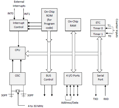
This architecture can also be shown in the form of block diagram as

There are totally 21 SFRs , of which 9 were discussed in brief.
You can also refer this for 8051 architecture
Also read:
