
Pin diagram of 8051 microcontroller
In this tutorial, A brief description on pin diagram of 8051 microcontroller and in upcoming tutorials , each pin will be explained in detail.
XTAL1 , XTAL2:

These two lines are connected to a quartz crystal. Once the power supply is given to Vcc , this starts oscillating and gives a clock signal. Clock signal basically triggers the processor. This is basically a 12MHz frequency oscillator.
Why does a microcontroller need a clock ?
Processor keeps on performing tasks one by one, But the question comes, when does it perform the next activity. Continuous triggering will remind it to perform tasks. It changes the state of the processor. Higher the triggering, higher is the state changing of the processor, which leads to more speed. If these pins are absent, the processor would perform one action ( only a single instruction ) and stop.
RESET:
Whenever this pin is set for HIGH, the whole power supply is withdrawn and given back. It means RAM will be cleared. On reset, the processor executes a program named BIOS ( basic input output system ) also known as monitor program. It will be explained in upcoming tutorials.

Arrow shows that RST is the signal given to the 8051 and decided by the user.
ALE:
ALE stands for address latch enable.
8051 has 16-bit address buses and 8-bit data buses. However address and data buses aren’t used parallely, first address bus fetches address of the target, then data bus comes into picture.
A7 – A0 are lower order address buses and A15 – A8 as higher order address buses.

As a result address lines and data lines are multiplexed. So work of 16 lines is done by 8 lines, these lines are AD7 – AD0. So overall there are 16 lines instead of 24 lines. 8 lines for address bus and 8 lines for both address and data bus.
3000 is also an address and also data, so whether it is data or address, this is shown by ALE pin. If ALE=1, then it is address or else data.

Arrow shows that, ALE signal is given and decided by the processor.
EA ( EA bar ):
It is pronounced as EA bar and it stands for external access also known as enable external access. Every microcontroller has internal RAM and ROM, and which is always expandable upto a limit. This limit is decided by the number of address lines. Here there are 16 address lines which means
Expandable memory = 216 = 26 x 210 = 64 kilo bytes.
For other processors such as 8085,8086 this is the total ( RAM + ROM ) expandable memory, But in the case of 8051 it is the memory expandable for RAM as well as ROM. RAM can be expanded more 64KB and ROM too.
Now there stands internal RAM and external RAM , same in the case of ROM. There is something by which internal RAM and external RAM work separately, they don’t interfere ( these all things would be explained in upcoming tutorials ). And internal ROM and external ROM can work together , they can get combined to work. Suppose we want to remove internal ROM and work only with external ROM then EA bar= 0.

If EA bar is set to ‘zero’ , then the base addressing will start from the external ROM. Simply internal RAM would not be used.

EA bar is the signal given to 8051 and decided by the user. This was some part of pin diagram of 8051 microcontroller , and rest are listed below.
Vcc, GND:
These are the power supply and grounding given to 8051. It is 5V.

RxD , TxD ( serial port ) :
These are the two pins for serial communication to transfer and receive data. TxD is for transferring data serially and RxD is for receiving data serially.

INT0 and INT1:
These are interrupt pins. Let’s consider processor is busy in doing it’s duty, and suddenly there caused a problem ( actually not a problem ) , then that part of the system sends int ( interrupt ) to the processor , and processor stops it’s duty and goes to a new program ISR ( interrupt service routine ) [ program to solve the issue ], then processor comes back and continues its duty. ISR is a solution to an interrupt. To read more about interrupts , click here
There are two interrupt pins INT0 and INT1, if both of them sends interrupts at same time, then there is an inbuilt priority order ( order can be changed using SFR) , by inbuilt first priority is given to INT0.
E.g: Let’s assume we are watching a video in youtube ( Processor’s duty is to run video ) , then suddenly a phone call comes, then processor pause the video and goes to that action and solves the issue ( here solving is lifting the call, ignoring or something else ) , once the call is over ( interrupt is solved ) , then processor comes back and resumes video.

INT0 and INT1 are the signals given by other parts to the processor.
T0 and T1 :
These are the timer pins. Already discussed the timer in the previous tutorial. For a timer , to run it needs a clock signal, so separate clock signals are required. Timers, interrupt, serial pins are important part of pin diagram of 8051 microcontroller .To read more about timers , click here
Why can’t we use the 12MHz clock for timers?
8051 has 16 bit counters which can count upto 65,535 and the frequency of oscillator is 12MHz which is 12 million counts per second, if this is used for timers as clock signal then these timers can count for 0.00546125secs. So for every 0.00546125 timer will send signal to processor that “ counting is done “

WR and RD:
These are the commands given by the processor. If RD= 0 , then it means the processor wants to read the data.

PSEN :
pin diagram of 8051 microcontroller has PSEN which stands for program store enable. In the EA bar pin we have discussed internal and external RAM, ROM. If 64KB external memory is attached externally then both RAM and ROM has same address, if there is an instruction to access data of address ‘2200’ , this address is present in external RAM as well as external ROM. So if
WR and RDare activated then action should be performed on RAM
PSEN is activated then action is performed on ROM, as PSEN gives only read feature because ROM is read only memory.
PORTS:
There are four ports P0, P1, P2, P3 ( each port has 8 lines ) and all the 32 lines are bidirectional ( can act as input as well as output ). All the lines are bit addressable ( can be controlled individually )
Connect 8 LEDs with 8 lines of P0 , it would act as an output port.
Connect 8 keys with 8 lines of P0 , it would act as an input port.
So till now we have discussed more than 10 pins and then these 32 pins, its sums to be 42+ pins. But 8051 has only 40 pins???
P0, P2, P3 has alternate ports.
P0 has those multiplexed pins ( address and data lines ) from AD0 – AD7
It means P0 can be used as an I/O port or as these alternate buses.
P1 has no alternate ports, it has purely 8 I/O lines.
P2 has A15 – A8 address buses.
P3 has other alternate serial ports, interrupt ports, timers and read,write pins.
Why these alternate pins??
Generally address buses select the address of the memory for data transfer, and in microcontroller all the memory is embedded in a single chip, so address lines are not used until any external memory is attached. In 90% of cases we don’t use external memory in a microcontroller ( we don’t put memory cards in a washing machine ). So there is no use of those address buses in most of the cases. And if there were separate ports for the address bus, it would have been a great loss ( commercially , size wise ) .
COMPLETE PIN DIAGRAM OF 8051 MICROCONTROLLER:

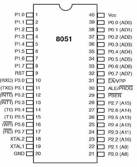
This was all about pin diagram of 8051 microcontroller.
Check data sheet of 8051 microprocessor
Also Read:
8051 microcontroller architecture